Humanism
Solitude Is Not a Curse: The Danger of Pathologizing Being Alone
29 March 2026
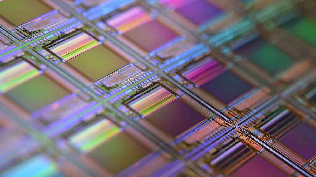
Imagine electrical circuits so tiny you can’t see them with the naked eye. Record-small microchips are the work of researchers at Johns Hopkins University. Their discovery could usher in a new era of miniaturization in electronics — powered by record-small microchips.
Can we build electrical circuits smaller than anything we’ve known so far? That was the goal set by a team at Johns Hopkins University (JHU). Their discovery, published in the prestigious journal Nature Chemical Engineering, opens the door to manufacturing circuits at sizes that not long ago seemed impossible. Will record-small microchips soon find their way into our computers and phones?
“Companies have roadmaps for where they want to be in 10 to 20 years and beyond,” explains Michael Tsapatsis, professor of chemical and biomolecular engineering at JHU and a co-author of the discovery, in an interview with Phys.org. “One obstacle has been developing a process to make smaller features on the production line, where you can irradiate materials quickly and with absolute precision.” The JHU scientists set out to change that.
Microchips are flat pieces of silicon with printed circuits that perform core functions. In fabrication, the manufacturer coats silicon wafers with a radiation-sensitive material, creating an ultrathin layer called a resist. During exposure, when a beam is directed at the resist, it triggers a chemical reaction that etches circuit details into the wafer.
The problem arises when you push for ever smaller features. Higher-intensity beams needed to sculpt the tiniest elements don’t interact strongly enough with traditional resists. This is where the Tsapatsis team’s breakthrough comes in.
Worth reading: Japanese Breakthrough: Thanks to Extraordinary Caterpillars
Crucially, earlier work showed that resists made with certain materials can work with beyond extreme ultraviolet (B-EUV) irradiation. The approach has the potential to create features smaller than today’s 10-nanometre standard. “By using two components (a metal and an imidazole), you can tune light absorption and the follow-up chemistry,” Tsapatsis explains. He notes there are at least 10 different metals and hundreds of organic compounds that can be used in this process.
The JHU researchers developed a methodology that enables precise fabrication and fast exploration of different metal–imidazole combinations — opening up near-endless optimisation. “Because different wavelengths interact differently with different elements, a metal that ‘loses’ at one wavelength can be a ‘winner’ at another,” says Tsapatsis. “Zinc isn’t great for extreme ultraviolet (EUV) radiation but it’s among the best for B-EUV.”
Does this mean that in a decade we’ll carry devices in our pockets with the power of today’s supercomputers? One thing is certain: the limits of miniaturisation have just moved much further — thanks to record-small microchips.
Read this article in Polish: Nowa era miniaturyzacji. Powstały rekordowo małe mikrochipy


A journalist and a graduate of Jagiellonian University. He gained experience in radio and online media. He has dozens of publications on new technologies and space exploration. He is interested in modern energy. A lover of Italian cuisine, especially pasta in every form.


Zmień tryb na ciemny